← How to Install Solar Panels on Roof: The Complete Beginner's Guide Premium photo Apex Amplifier Circuit Diagram: Build the Simplest Amplifier with Ease! apex legends 'shockwave' gameplay trailer released →
If you are searching about Step-by-step cadence PCB design tutorial - RayPCB you've visit to the right page. We have 25 Pictures about Step-by-step cadence PCB design tutorial - RayPCB like KiCad-Tutorial-for-PCB-Design-and-Routing | Maker Cube Events, KiCad EDA Schematic Capture PCB Design Software, 41% OFF and also KiCad PCB Design Step-by-Step Tutorial for Beginners - TechSparks. Here it is:
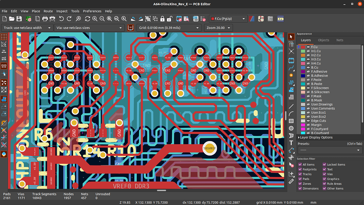
Step-by-step Cadence PCB Design Tutorial - RayPCB
 www.raypcb.com
Step-by-step cadence PCB design tutorial - RayPCB
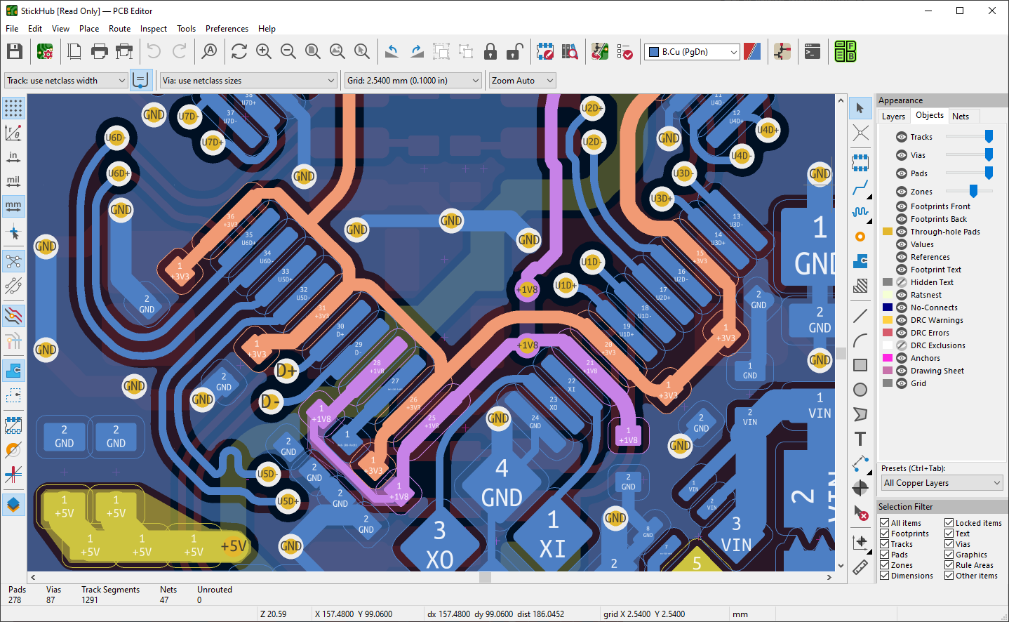
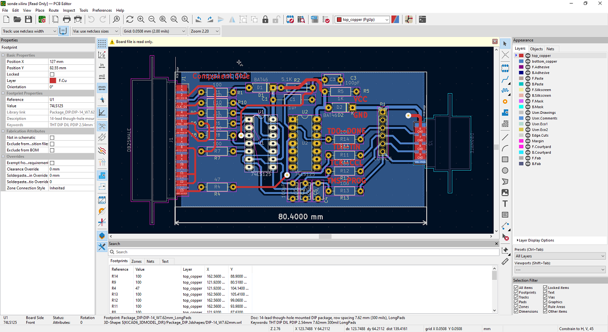
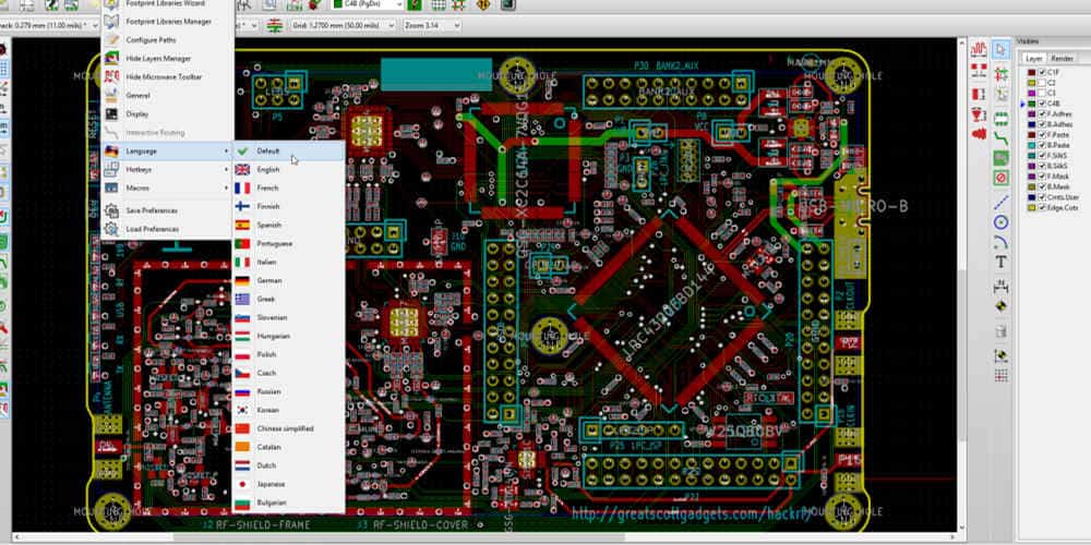
How To Make Pcb In Kicad At Vera Malone Blog
 storage.googleapis.com
How To Make Pcb In Kicad at Vera Malone blog
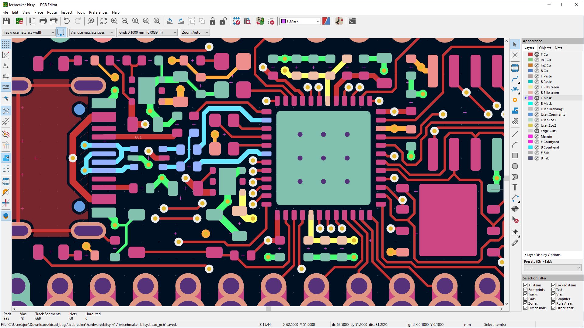
How To Get Your KiCad PCB Design Ready For Fabrication – KiCad Version
 circuitstate.com
How to Get Your KiCad PCB Design Ready for Fabrication – KiCad Version ...
Introduction To Basics Of Kicad PCB Design – Hillman Curtis: Printed
 hillmancurtis.com
Introduction to Basics of Kicad PCB Design – Hillman Curtis: Printed ...
KiCad Version 6.0.0 With New Interface And Improved PCB Design
 www.electronics-lab.com
KiCad Version 6.0.0 with New Interface and Improved PCB Design ...
KiCad EDA - Schematic Capture & PCB Design Software
 www.kicad.org
KiCad EDA - Schematic Capture & PCB Design Software
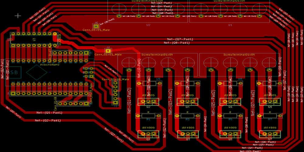
KiCad PCB Layout Quick Tips - Embedded Computing Design
 embeddedcomputing.com
KiCad PCB Layout Quick Tips - Embedded Computing Design
Pcb Layout Design Tutorial Pcb Design & Layout
 circuitschematics.z20.web.core.windows.net
pcb layout design tutorial Pcb design & layout
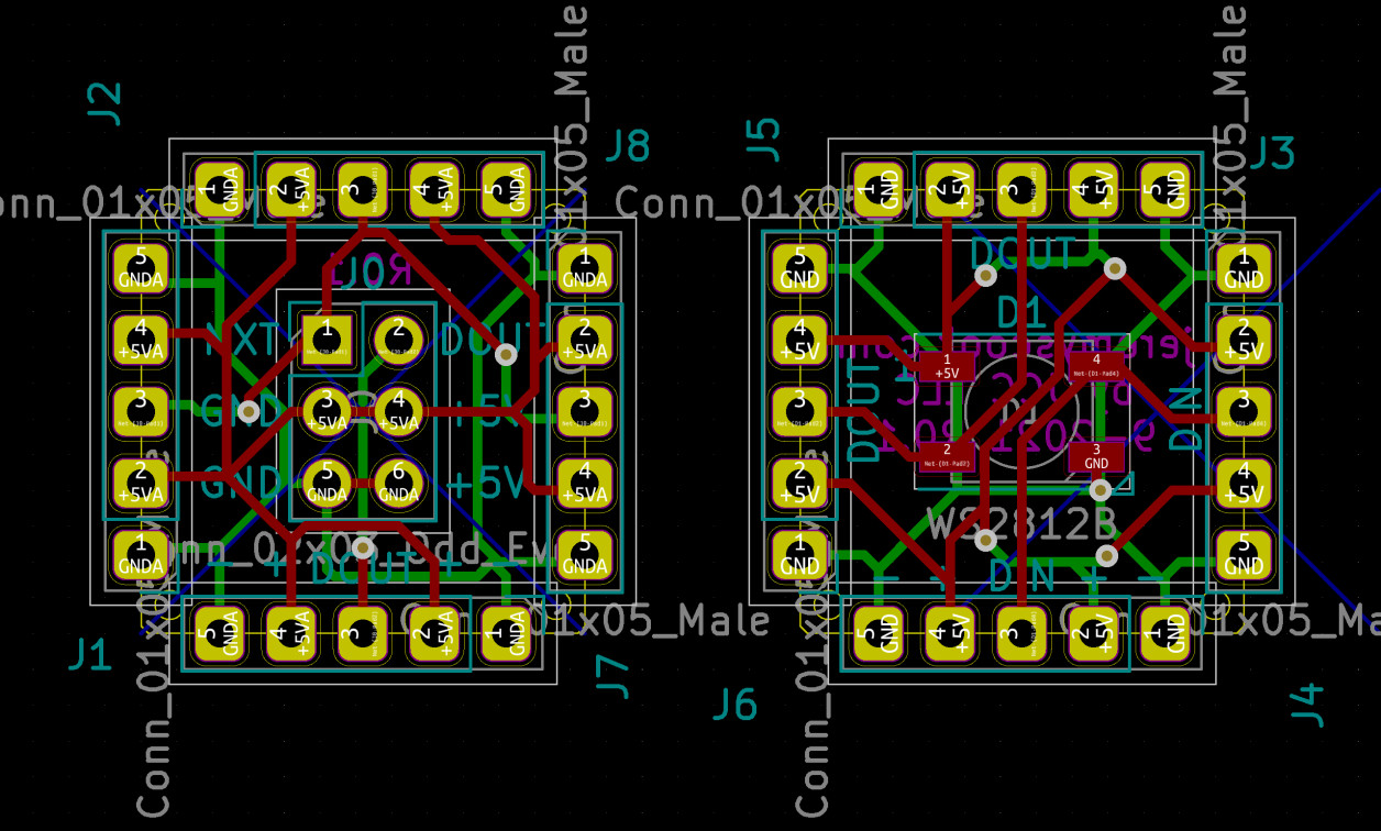
How Do I Convert A Schematic To PCB Layout In KiCad (Step By Step) - RayPCB
 www.raypcb.com
How do I convert a Schematic to PCB Layout in KiCad (Step By Step) - RayPCB
KiCad 6 STM32 PCB Design Full Tutorial - Phil's Lab #65
 www.fedevel.com
KiCad 6 STM32 PCB Design Full Tutorial - Phil's Lab #65
How To Make Pcb With Kicad Pcb Designs - Vrogue
 www.vrogue.co
How To Make Pcb With Kicad Pcb Designs - Vrogue
KiCad EDA Schematic Capture PCB Design Software, 60% OFF
 elevate.in
KiCad EDA Schematic Capture PCB Design Software, 60% OFF
How To Get Your KiCad PCB Design Ready For Automated Assembly – KiCad 6
 circuitstate.com
How to Get Your KiCad PCB Design Ready for Automated Assembly – KiCad 6 ...
KiCad EDA Schematic Capture PCB Design Software, 50% OFF
 www.micoope.com.gt
KiCad EDA Schematic Capture PCB Design Software, 50% OFF
KiCad EDA - Schematic Capture & PCB Design Software
 www.kicad.org
KiCad EDA - Schematic Capture & PCB Design Software
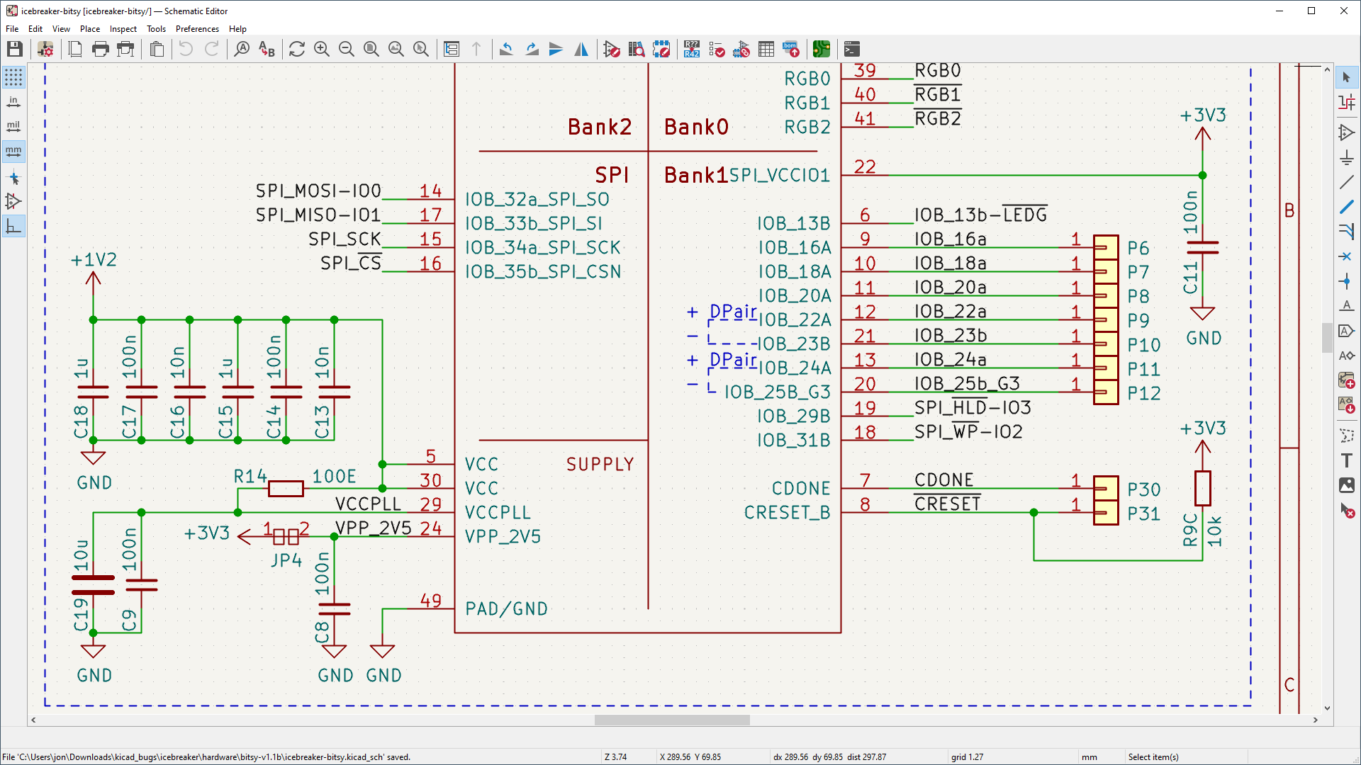
KiCad-Tutorial-for-PCB-Design-and-Routing | Maker Cube Events
 events.makercube.ca
KiCad-Tutorial-for-PCB-Design-and-Routing | Maker Cube Events
KiCad EDA Schematic Capture PCB Design Software, 41% OFF
 www.bharatagritech.com
KiCad EDA Schematic Capture PCB Design Software, 41% OFF
KiCad PCB Design Step-by-Step Tutorial For Beginners - TechSparks
 www.tech-sparks.com
KiCad PCB Design Step-by-Step Tutorial for Beginners - TechSparks
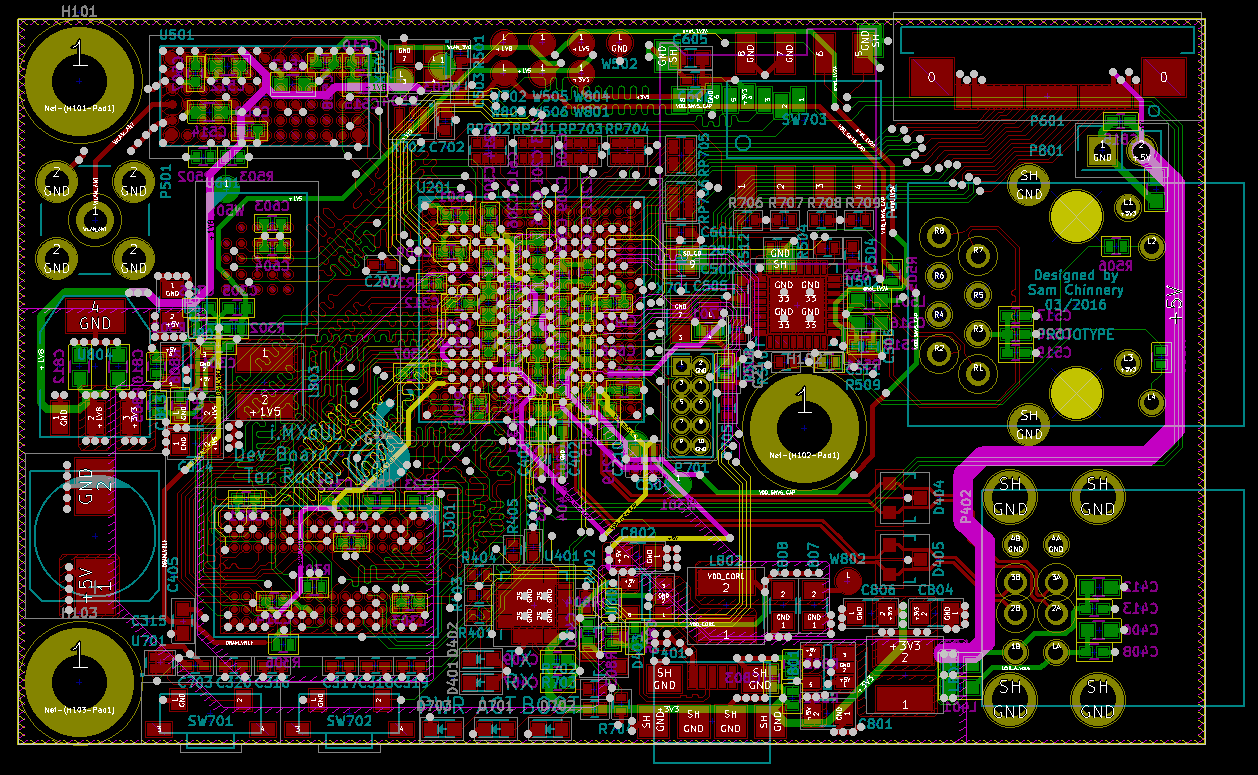
Kicad 2 Layer PCB Design: Tips And Best Practices – Hillman Curtis
 hillmancurtis.com
Kicad 2 Layer PCB Design: Tips and Best Practices – Hillman Curtis ...
Failed To Load Pcb Layout Expecting ‘(’ In .kicad_pcb" File Line 1752
 forum.kicad.info
Failed to load pcb layout expecting ‘(’ in .kicad_pcb" file line 1752 ...
Kicad 2 Layer PCB Design: Tips And Best Practices – Hillman Curtis
 hillmancurtis.com
Kicad 2 Layer PCB Design: Tips and Best Practices – Hillman Curtis ...
KiCad EDA - Schematic Capture & PCB Design Software
 www.kicad.org
KiCad EDA - Schematic Capture & PCB Design Software
KiCad PCB Layout Quick Tips - Embedded Computing Design
 embeddedcomputing.com
KiCad PCB Layout Quick Tips - Embedded Computing Design
KiCAD 7 PCB Layout In 5 Steps | Circuit, Steps Youtube, Layout
 www.pinterest.com
KiCAD 7 PCB Layout in 5 steps | Circuit, Steps youtube, Layout
Kicad Electrical Wiring Diagram - Wiring Work
 www.wiringwork.com
Kicad Electrical Wiring Diagram - Wiring Work
kicad eda schematic capture pcb design software, 50% off. Kicad 2 layer pcb design: tips and best practices – hillman curtis. kicad electrical wiring diagram